
Abstract:
This paper aims to emphasize on the importance of integrating design for failure analysis in the layout considerations during the IC development process. It will have a brief overview on the importance of failure analysis in an IC development process, followed by an understanding of the failure analysis methodologies in the industries. This leads us to the different considerations in the layout of ICs to facilitate failure analysis, and also the challenges in failure analysis with increasing complexities when the design approaches nano-electronics.
I. INTRODUCTION
The introduction of the System-on-a-Chip (SOC) and the increasing complexity of ASIC designs has made testability and analysis of Integrated Circuits (IC) more challenging. It has almost become a mandatory requirement to do a Design-for-Testability (DFT) and Design-for-Analysis (DFA) before the freezing of the ASIC design as the ability to test and analyze a complex design will bring about a shorter product cycle and faster time-to-market. In DFT, testability requirements are presented in various levels of an SOC. In terms of failure analysis, there are many techniques available to analyze the device for physical defects, from isolate the faulty behavior to the failing transistor and to capture the images at localized root cause in substrate level to understand the failing root cause. Unfortunately, even though there are many existing techniques available for failure analysis, the analysis may not always be possible. This is because the inevitable trend in IC design is that most of the time, in order to have a faster time to market, IC designers need to embed cores that are untested and are not manufactured in-house. There are inadequate considerations in the IC layout that make analyzability of an IC difficult or impossible. Furthermore, smaller technology nodes also brings about an increase in the metal layers of an IC, new materials in wafer manufacturing processes and different IC packages which pose greater challenges to failure analysis. These challenges lead to higher equipment cost, more experienced manpower required, longer analysis turn around time and difficulties in the analyzability of an IC. Even for reused IP which are proven in the design, process shrinking or backend process parameters shift may bring problems like higher leakage current and reduced reliability. Hence there is an increasing need to integrate failure analysis requirements with the IC development in an early phase. Strong interactions between development team and failure analysts are required to identify the possible bottlenecks from the very beginning and provide solutions with adequate layout considerations.
II. FAILURE ANALYSIS – THE DIFFERENT METHODOLOGIES
Failure analysis for integrated circuits is increasingly important and very much required for today’s complicated packaging and technology strategies. It is a process which requires the combination of analysis experiences, leading-edge equipment and techniques, and well defined failure analysis procedures to achieve fast turn around time for failure root cause findings. Failure analysis methodologies are important to the IC development process as it allows one to effectively identify the root cause of a design or process bug. The challenge of making rapid improvements in IC design and technology also requires the development of relevant failure analysis techniques. There are many analysis techniques and they can be generally divided into the 3 areas:
1. Chemical or physical preparation of the integrated circuits.
2. Fault localization of integrated circuit’s failing behavior.
3. Fault imaging of integrated circuits.
Chemical or physical preparation of the integrated circuit is the first step in the analysis of failing devices. The package has to be opened up either on the front or backside so as to allow further localization techniques to be carried out. Improved packaging techniques like Ball Grid Array (BGA) packaging had make the chemical or physical preparation increasingly challenging for failure analysis. This is an important process whereby one has to be careful not to destroy the failing signature and the electrical functions of a device.
Fault localization is the process where various techniques are used to isolate the defective areas on the die. Techniques like photoemission microscopy uses faint Infra-red radiation emitted by leakage current to localize the leakage site. Other techniques such as Thermal Induce Voltage Alteration (TIVA) uses the active approach whereby failure sites are located use a scanning ionizing beam, such as laser beams, to stimulate failures that are sensitive to carrier generation or thermal stimulation.[1] This allows one to reduce the area required for analysis and significantly save on the time required for failure analysis. The localized defect is then characterized with a view to understand the failure mechanism.
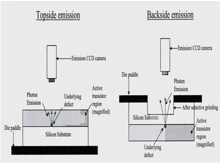
Fig. 1. Top and bottom photoemission setup in fault localization
The final step of failure analysis after fault localization is fault imaging. Failure analysis can only be completed once the root cause of the failure has been identified. Hence the defect must be imaged to prove the defective behavior. Optical microscopy is the obvious and most basic equipment for this purpose. However, with the complexity of microelectronics today, optical microscopy is of limited use. In order to achieve better resolution for imaging, microscopy is available using all kinds of beams: ultrasonic, electromagnetic (from infrared to x-ray) and particles like electrons and ions or near-field interactions with a stylus, as in scanning probe microscopy. All these imaging tools are equipped with CAD layout information for better navigation over the die. The FA processes can be generally summarized in the following table
...

 The total does not include foundry sales.